Environmental and Airflow Control Systems in Leading Semiconductor Fabs
Precision control of humidity, static, and out-gassing is critical in advanced semiconductor fabrication facilities. Tight humidity control within ±1% RH prevents wafer warping and process instability in high‑precision lithography applications. Advanced foundries utilize condensation control systems to maintain stable humidity levels, paired with ionized air solutions to minimize static risks for 300mm wafers. Multi‑stage chemical scrubbers effectively control photoresist out‑gassing, supporting high yield performance in EUV lithography processes.
HEPA / ULPA Filtration & Cleanroom Infrastructure Support
Advanced semiconductor fabs rely on high‑density HEPA and ULPA filtration systems to achieve ISO 3–5 cleanroom conditions, with ultra‑high efficiency for particles down to 0.12 microns. Cascading and laminar airflow designs enable high air‑change rates required for sub‑7nm and 3nm/5nm node manufacturing.
The structural integrity and stability of these filtration systems depend heavily on rugged, cleanroom-compatible support frameworks. Hengdong Aluminum specializes in cleanroom‑grade aluminum profiles and structural solutions that serve as the foundational framework for FFU (Fan Filter Unit) mounting, filter housings, and cleanroom ceiling grids. Our rigid, corrosion‑resistant aluminum structures ensure consistent airflow distribution and long‑term dimensional stability for critical filtration environments.
Real‑time Monitoring & Environmental Control Systems
Leading fabs deploy thousands of wireless sensors for real‑time monitoring of particles, vibration, pressure differential, temperature, and humidity. Rapid feedback loops enable automatic HVAC adjustment to maintain strict environmental parameters, directly supporting high yield rates in advanced wafer production.
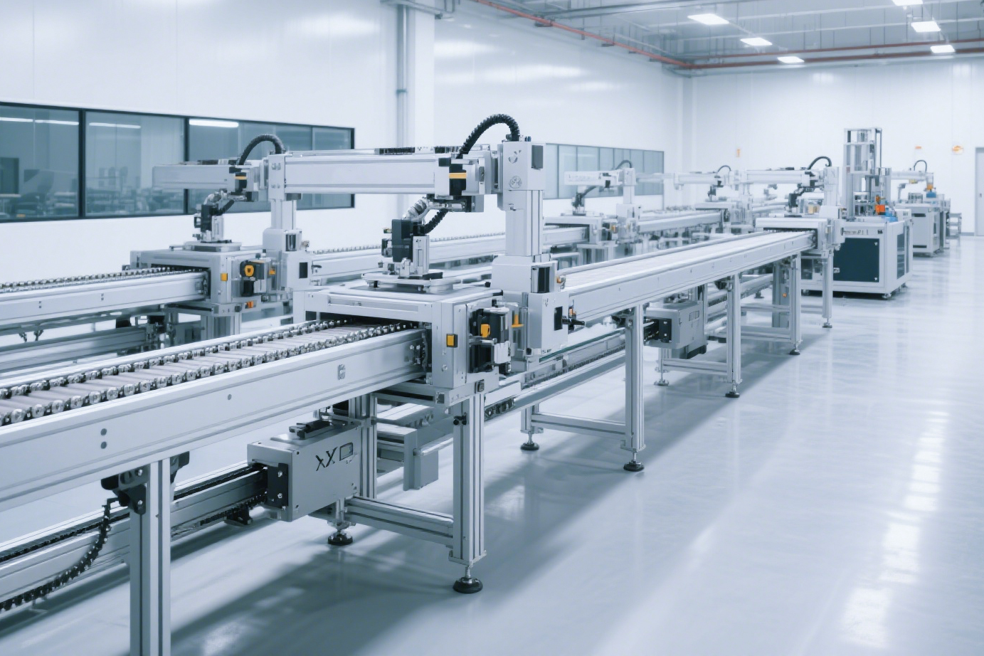
These monitoring sensors and control devices are often installed on modular aluminum framing systems that allow flexible positioning, easy maintenance, and future reconfiguration. Hengdong Aluminum’s linear systems and structural profiles provide a lightweight yet high‑strength platform for mounting sensors, cabling trays, and environmental control components without compromising cleanroom integrity.
Cleanroom Classifications & Standards in Semiconductor Manufacturing
Semiconductor cleanrooms follow stringent ISO 14644‑1 and SEMI standards, requiring ultra‑low particle counts for lithography, deposition, and other critical processes. Even minor contamination can result in significant yield loss, making stable, contamination‑resistant infrastructure essential.
Structural & Enclosure Solutions for Semiconductor Cleanrooms
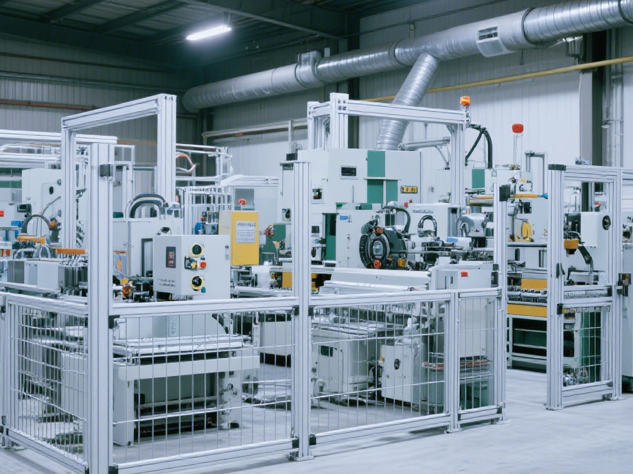
Beyond airflow and filtration, the physical envelope of the cleanroom plays a vital role in long‑term performance. Hengdong Aluminum provides industry‑leading cleanroom aluminum profiles, wall framing systems, modular panel mounting structures, and equipment support racks designed specifically for semiconductor‑grade environments.
- Cleanroom‑grade aluminum extrusion with smooth, non‑shedding surfaces
- Structural frameworks for cleanroom walls, ceilings, and partitions
- Custom racks and supports for process tools and handling systems
- Modular, reconfigurable designs to adapt to evolving fab layouts
Our Cleanroom‑Grade Aluminum product series meets the strict dimensional and hygienic requirements of semiconductor facilities, minimizing particle entrapment and supporting long‑term operational stability.
Air Changes, Filtration Efficiency & Structural Dependencies
High‑end semiconductor cleanrooms require extremely high air‑change rates and ULPA filtration performance. These demanding engineering specifications rely on durable, dimensionally stable support structures to maintain filter alignment, airflow uniformity, and pressure containment.
Hengdong Aluminum extrusion systems deliver:
- High strength‑to‑weight ratio for overhead FFU and filter support
- Excellent corrosion resistance and cleanability
- Precision tolerances for modular panel installation
- Compatibility with ISO 14644 and SEMI‑recommended cleanroom design practices
Emerging Trends: Flexible & Modular Cleanroom Infrastructure
Next‑generation semiconductor fabs are moving toward modular, reconfigurable cleanroom designs to accelerate tool upgrades, layout adjustments, and new process validation. Key trends include modular panels with integrated IoT capability, digital twin simulation, and faster cleanroom qualification cycles.
This shift strongly favors flexible aluminum structural systems over traditional welded steel or fixed construction. Hengdong Aluminum enables this agility through:
- Modular framing for fast on‑site assembly
- Reusable profiles that reduce waste and cost
- Compatibility with cleanroom wall panels and ceiling systems
- Customized linear systems for automated handling and tool integration
How Hengdong Aluminum Supports Semiconductor Cleanroom Excellence
As a professional manufacturer of industrial aluminum profiles and linear motion systems, Hengdong Aluminum provides critical structural and mechanical infrastructure for semiconductor cleanrooms:
- Cleanroom wall & ceiling framing
- FFU and filter mounting supports
- Equipment frames and machine bases
- Modular cleanroom enclosure structures
- Cleanroom‑compatible linear systems and guiding components
Our products form the invisible but essential backbone of HVAC, filtration, sensor, and environmental control systems in high‑performance fabs.
For more information about our cleanroom aluminum solutions and customized structural systems, please visit
hengdongaluminum.com or contact our engineering team for project support.